Material Characterization
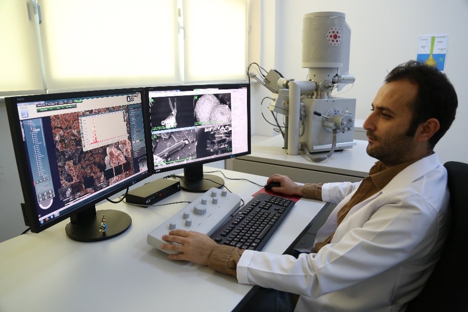
Scanning Electron Microscope (SEM)
FEI QUANTA FEG 250
It gives information about the topography and composition of the material. It can take measurements in three different vacuum modes: low / high vacuum and ESEM. Besides examining the surface morphologies of materials, it can also perform element (EDS (EDAX)) analysis.
 |
|
X-ray Diffraction Laboratory (XRD)
BRUKER D8 ADVANCE TWIN-TWIN
X-ray crystallography is a method based on the diffraction of the rays in the X-ray beam of crystallized atoms in various directions specific to the crystal. Powder, thin film, bulk materials can be analyzed. In addition, measurements can be made depending on stress and temperature (0 - 1300 °C).
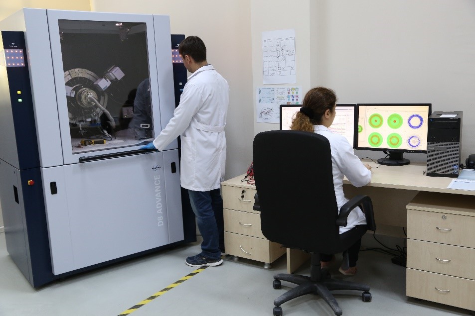 |
Three different sample trays are used in the multi-purpose X-Ray Diffractometer. - Powder diffraction trays - Temperature dependent measuring trays - Inclined trays (three axis as Chi, Phi, z) |
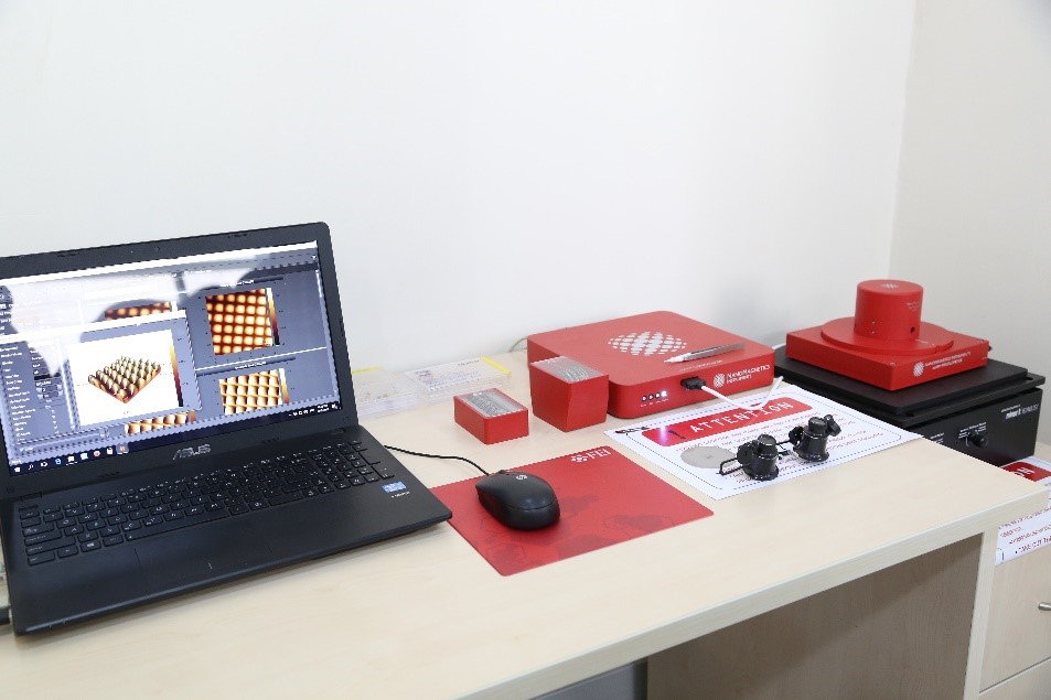
Atomic Force Microscopy Laboratory (AFM)
ez-AFM Nanomagnetics
Atomic force microscopy examines the 3D surface morphology of materials at high resolutions. The maximum resolution achieved is at the nanometer scale and is at least 1000 times more sensitive than optical techniques.
In addition to examining the surface morphology with the AFM device, it can also detect the coating thickness of the materials using Profilometer Mode.
 |
|
Electro-Optical Characterization Laboratory
CRYO In. (Sumitomo) / Keithley / Solar Light /Agilent /Lake Shore / SP
It is used to analyze the electrical, magnetic and optical properties of materials.
 |
|